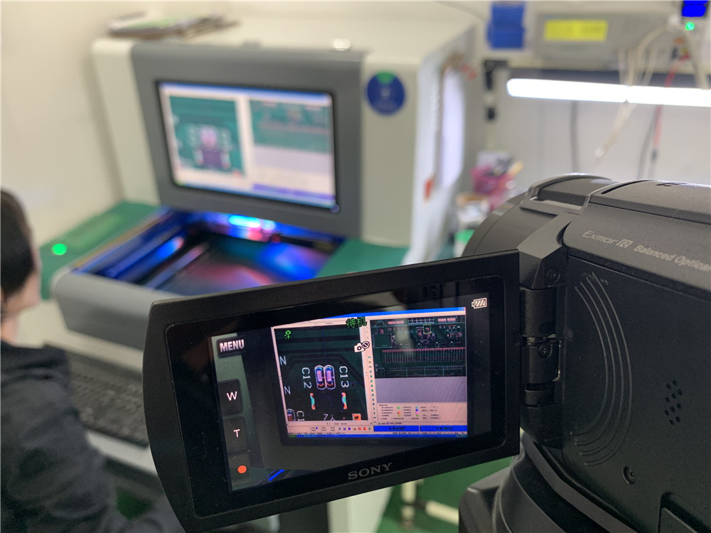
Today, we will expose the whole process of the PCB circuit board production; let us together enter into the production workshop of Hangzhou KinCony Electronics, to see how the circuit boards of the smart home device are produced and how the quality control is guaranteed.
In the magazine, it is mainly showing pictures and text data, actually, we also use 4k Sony high-definition camera to record the production details of every step. The video will be uploaded to the《Radio》 magazine platform, you can download it for watching.
Following are the production process of the “KC868-H32 Smart Control Box” , which was introduced in the previous issues “Rapid Development of Smart Home Systems” of magazine 《Radio》, let us see how it turned out to be a finished product from a spare part.
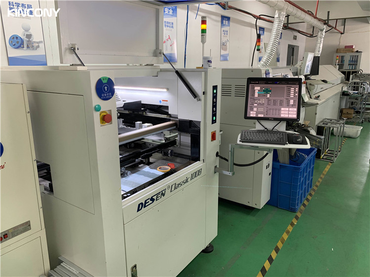
First, let’s have a look at the production line: in the patch stage, the production line of the circuit board is mainly composed of the automatic steel net paste machine, the automatic mounting machine and the reflow soldering equipment.

This is a fully automatic steel net solder paste machine.
When we design the circuit board, we usually make a steel mesh before production, which is used in this equipment. It is used to allow the machine to automatically tin the circuit board pad, just as we would like to use rosin when soldering.
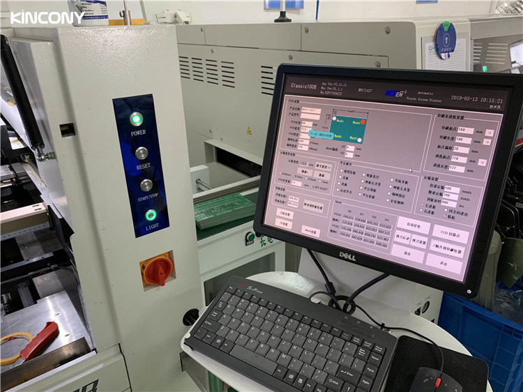
The computer can accurately position the coordinate of each anchor point. And set the dimensions of the steel mesh; including the exact coordinates of the X and Y axis.
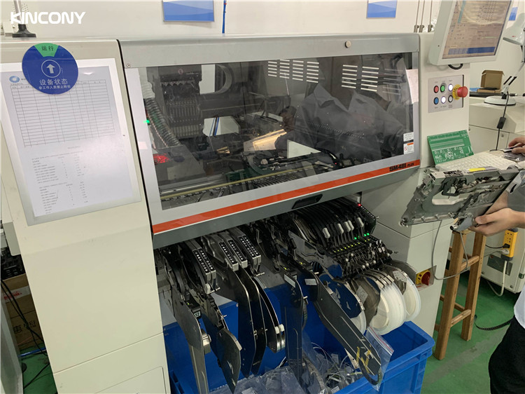
This is the fully automatic mounting machine, very fast to put each patch element neatly placed on the board of the welding pad. You can also think of it as a machine hand.

This is a reflow soldering device. After the patch elements are placed on the board, which will be sent to the device for soldering. You can think it as a bread oven.

These are the “KC868-H32” smart home control board to be prepared for processing

Very glossy PCB board empty board, now there is nothing on it.
In general, when it’s designed, we will add silk printing layer information on the PCB to identify the product name, model number and version number of the board, such as “KC868-H32 Relay Controller REV:2.1 Made By KinCony”, which indicates the manufacturer, the product name and the version number respectively. It’s also convenient to carry on the PCB board design update and maintenance in the future.

This is the programming settings for the surface mounting machine, which is based on the name and tag of the components on the BOM list of the PCB board.
What is a BOM list? It can be understood as a list of components exported by the hardware PCB design software, such as the Protel and AD. The list clearly records the name, tag, and package and quantity information of each component. And these information are inputted into the software system of the surface mounting machine, so that the machine will know what and where the components are, then put them in the right position in the fast state without any misplacement.

This is the software interface of the surface mounting machine, which has been finished to set up. It is already included the information of the BOM list. At the right bottom, it’s the real-time camera where the PCB can be accurately enlarged and viewed.

This is the software configuration for the full-automatic tin-paste printer.
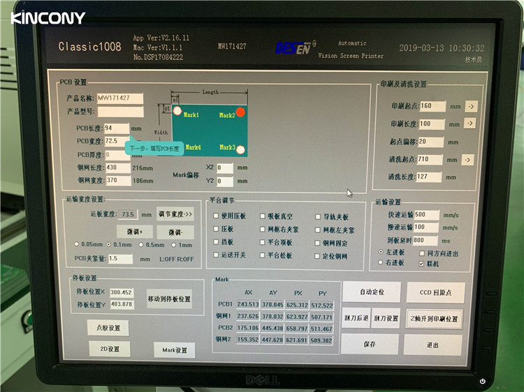
It is mainly used to accurately set the positioning parameters of the steel mesh, such as the size of the PCB board and the motion parameters of the mechanism.
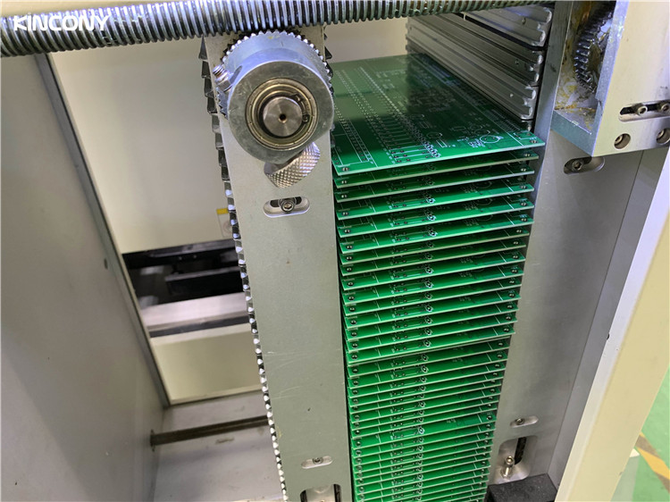
It is loading the empty PCB board into the feeder.
You can see there are many small grid drawers inside of the feeder; each empty PCB board is inserted into the grid.
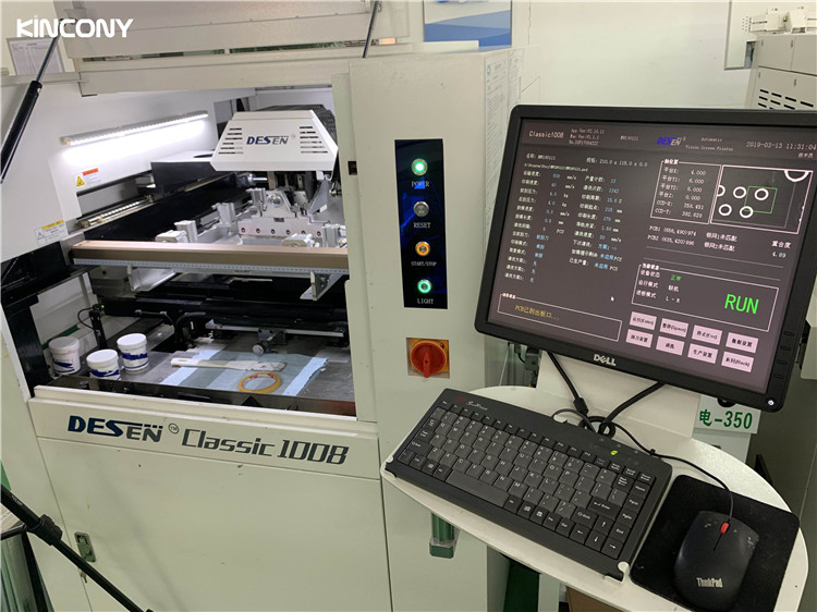
On the process of automatic tin by the machine, the computer can real-time monitor the process and browser the real-time production data.

All kinds of data are reflected on the screen.

The PCB board is automatically transferred to the steel mesh machine.

The steel mesh is on top of the PCB board, and the solder paste is automatically applied.
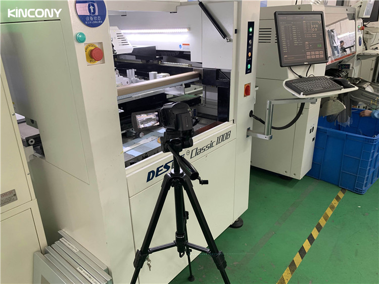
Our camera is facing the machine for real-time video capture. Readers and friends can also watch real-time videos through the website of 《Radio》
 +
+
After tinning, the PCB board will be automatically fed into the high-speed mounting machine for automatic patch. It will be very spectacular by watching the video.

This is the finished PCB board after surface mounting; as you can see, there are already a variety of patch components now.
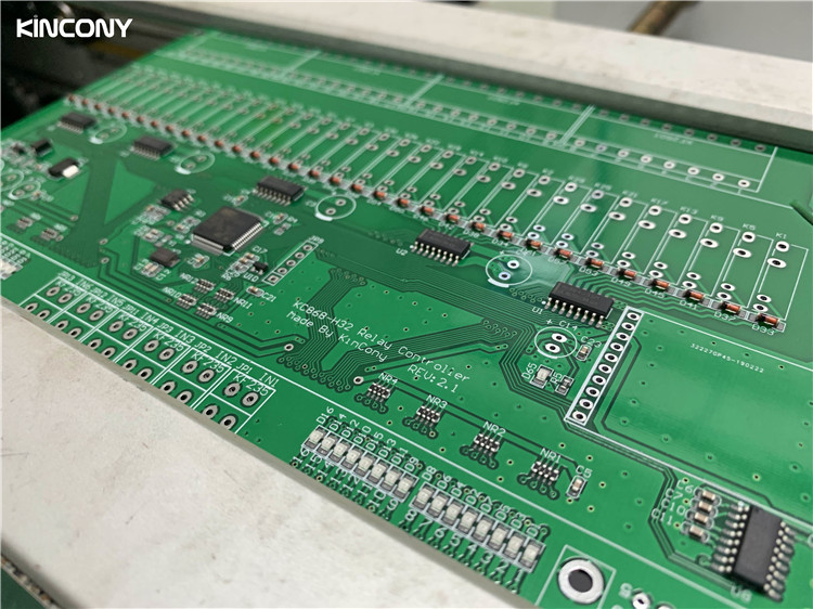
To have a look closely, it is very beautiful isn’t it? It is worthy of full automatic precision operation, very neatly.

From the outlet of the surface mounting machine, we can see the process line of the full-automatic solder paste printing machine from the former steps.
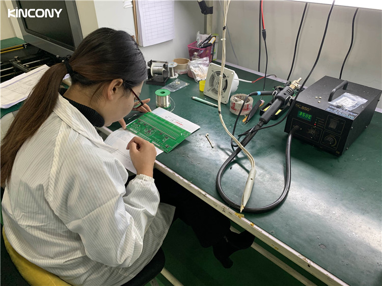
After finishing the welding of the first PCB board, manual inspection is required to confirm whether there is any setting error.

The electronic components on the PCB board are compared manually with each component in the BOM list. After there is no problem with manual alignment, the batch production of all PCB boards is then carried out.
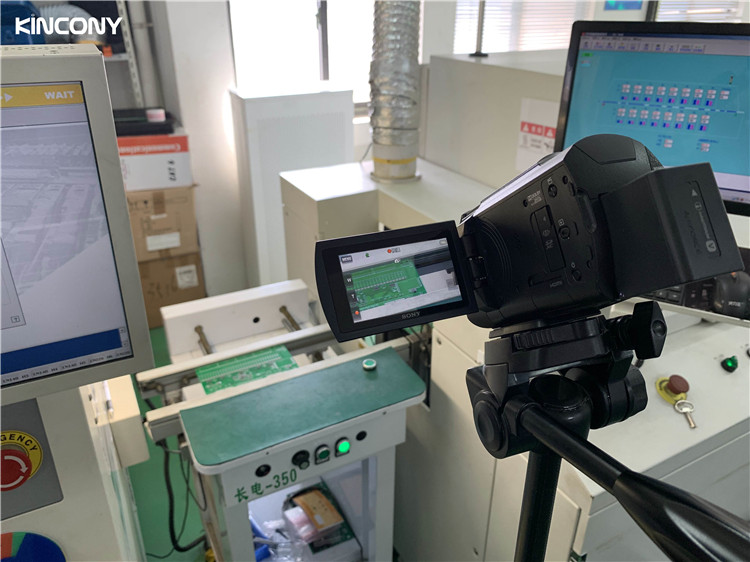
After the surface mounting is finished, the next step is “reflow soldering”. The function of reflow soldering is to heat the pins of the patch element and the PCB soldering board, and when the temperature is lowered, the solder paste soldering board will become solid. Because the PCB board delivered at the end of the mounting machine, in fact, all the equipment only stuck to the solder paste on the board, not really solidified, like building a house, cement, brick is the same thing. Bricks on the cement, before the cement, in fact, the brick can be moved, after the cement dry binding, the brick will be firmly fixed. “Reflow Soldering” played a role to let soldering paste solidify.

This is a PCB board from the “reflow soldering” machine. Like the bread comes out of the oven, it’s no longer flour. Now the PCB has been a solidified shape.
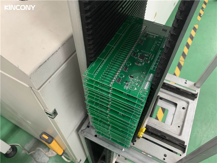
Automatic thruster will automatically push the PCB board out of the drawer for neatly placed. For this process, it’s recommended to watch video to learn.
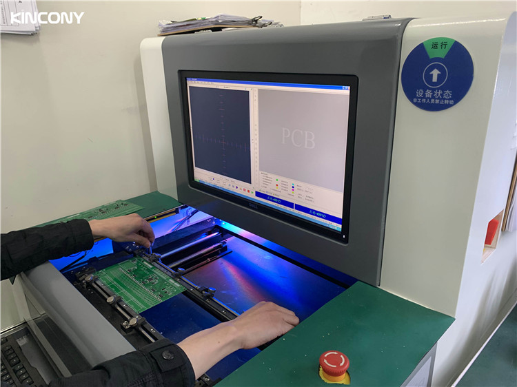
The PCB semi-finished board of the patch element is tested by AOI optics.
Let’s do some popularization of science; AOI is the abbreviated description of the “Automated Optical Inspection”, which is based on the optical principle to detect the common defects encountered in welding production. AOI is a new type of testing technology, but it has developed rapidly, and many manufacturers have introduced AOI testing equipment.
When the automatic detection, the machine automatically scans the PCB and capture images through the camera, and then the tested solder joints are compared with the qualified parameters in the database.
After image processing, the defects on the PCB are checked out, and display or mark the defect through screen or automatic mark for maintenance personnel to repair.
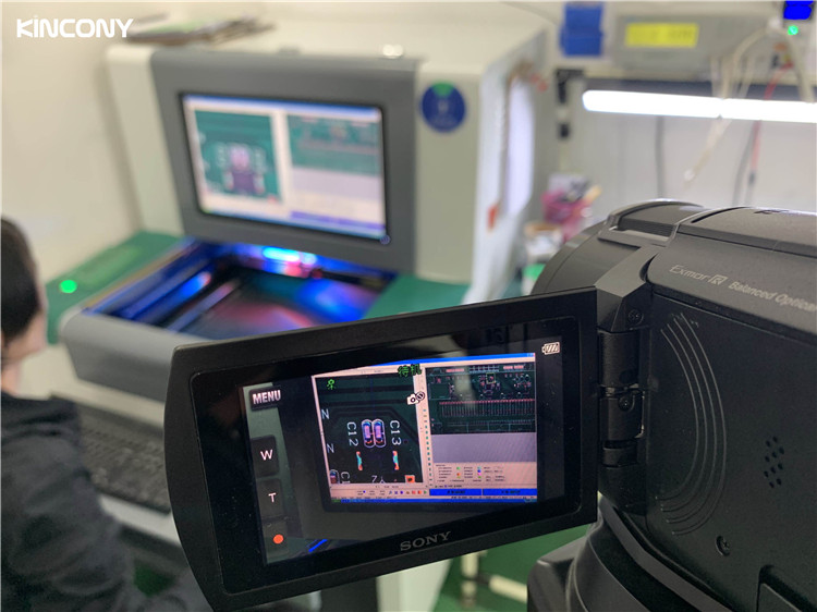
The AOI test program is written to optically scan each of the board on the PCB board.
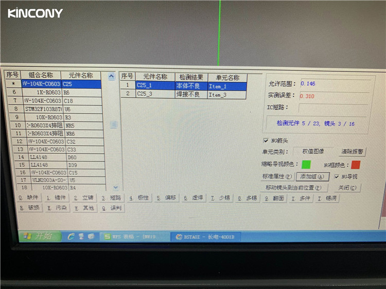
If a problem is detected, the computer will accurately locate a specific component and testing results for the operator to repair.

If after passing the full optical test, the computer screen displays the word “DONE”, meaning it is qualified.

At the end of the soldering process, we will do the welding work for the plug-in components. Because the volume of the plug-in components is large, and sometimes their shape is irregular, so it’s necessary to manually insert them into the PCB board and then do the soldering operation with “wave soldering”.
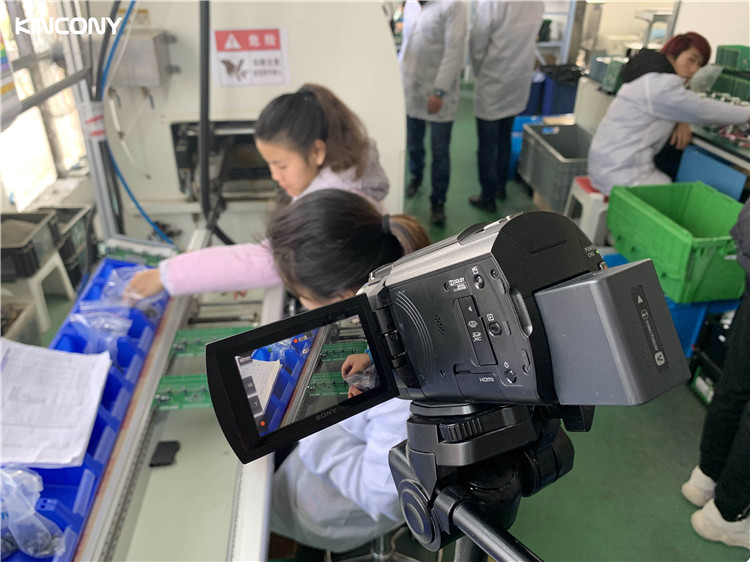
Workers put plug-in equipments, such as: electrolytic capacitors, connectors, relays and other mass equipment.
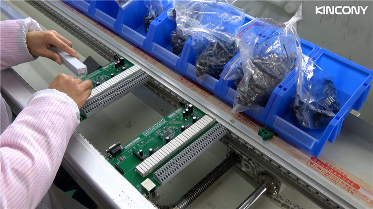
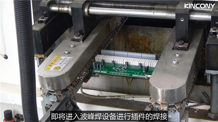
After the plug-in equipments are set up, the PCB board will be sent to the “reflow soldering” equipment for welding; and it will be used for automatic wine-spraying and welding operation.

Here is the “wave soldering” process, to do the science popularization of what is called “wave soldering.” It allows the welding surface of the board with plug-in components to contact directly with the high-temperature liquid tin for the purpose of welding. Its high-temperature liquid tin maintains a sloping surface, and a special device causes the liquid tin to form a wave-like phenomenon, so it is called “wave peak welding.” We can see the clear peaks of tin in the picture.
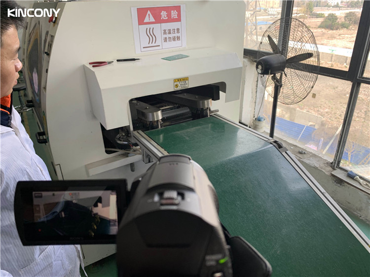
After the wave soldering out of the PCB plate, it is basically a formed circuit board.

At this time, we need to do part of the manual inspection and repair of the pad, and finally to test the software. Since then, all the welding process has been completed.

After testing the circuit board, we will assemble the shell.
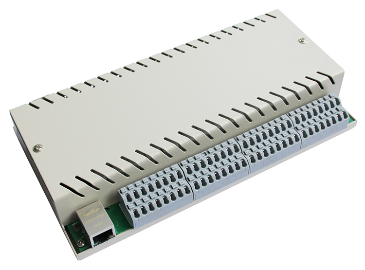
After assembling the shell, it is a set of finished products now.
After reading these photo albums, I believe that the production of the circuit board is not strange now; Because of the large number of pictures, the length of the article is limited, when you are interested, we strongly recommend watching the entire video process, the video have a caption description. More vivid, intuitive display of the “KC868-H32 intelligent control box” production process, we take the actual products as an example, so that we can understand the real manufacturers of the in-sale product production process and quality control process.

